
The application of Laser engraving machine in PCB industry-Ariel
The application of Laser engraving machine in PCB industry
This article is about the application of laser engraving machine in PCB industry.
The development of the intelligent 3C industry has led to the rapid development of the thin and light electronic industry. As the electronic component, the carrier PCB is especially important in the development of light and thin precision.
The thin and light development of PCB means that the area of PCB is getting smaller and smaller, the range of marking QR code is getting smaller and smaller, and the requirement for cutting precision is getting higher and higher.
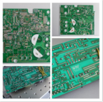
Printed circuit boards require some message. Barcodes, 2D and UID codes, serial number, batch numbers, and company information, logos, etc. Laser PCB marking is non-contact, no ink, no chemical and pollution, low running cost, permanent marking, good for the environment.
The advanced laser processing technology directly formed at one time. The non-contact processing has no burrs, high precision and high speed. In particular, the PCB will not cause damage to the components. By comparison, it can be seen that the traditional processing methods can not meet the ever-changing market demands such as narrower line width and narrower line spacing, smaller and smaller apertures, and higher flexibility. Advanced laser processing technology solutions are undoubtedly the best choice.
Contact us:Ariel Liu
Tel/whatsapp:0086 17866940010
Email:xintian122@xtlaser.com